
한양대학교 나노전자소자 및 재료연구실
Nano Electronic Devices & Materials Laboratory
본 연구실에서는 차세대 로직 소자, 메모리 소자, 뉴로모픽 소자 및 시스템, 3차원 집적 소자 분야에서 다양한 전자 재료, 반도체 공정 및 분석을 활용하여 연구를 수행하고 있습니다. 재료의 물리/화학적 특성을 이해하고 이를 바탕으로 반도체 소자를 제작하고 전기/광학/화학/물리적인 특성을 분석/해석합니다.
Our research activities consist of material, process, device and characterization for various advanced semiconductor devices in logic, memory, neuromorphic and monolithic 3D integration.
Our research activities consist of material, process, device and characterization for various advanced semiconductor devices in logic, memory, neuromorphic and monolithic 3D integration.
Recent News more
-
 [Lab Story] 차세대 반도체 산업을 이끌 기술 연구, NEDML2026-07-13
 -
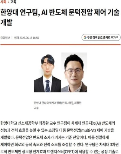 Symposium on VLSI Technology and Circuits 학회 발표!2026-07-13
Gallery more
-
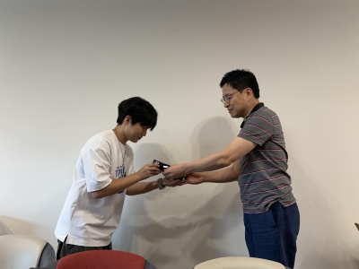 26년 2월 졸업생 감사패 수여식2026-08-06
 -
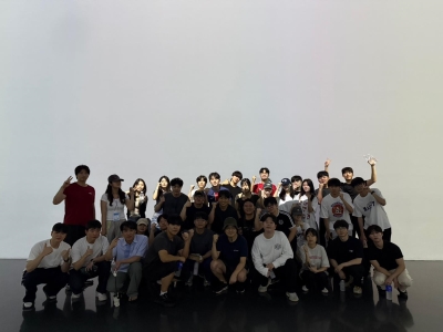 2026 반도체공학과 WORKSHOP2026-07-30
Journal more
-
Donguk Kim, Young Seo Na, Yehbeen Im, Kangbaek Seo, Seungchae Lee and Changhwan Choi*, "Plasma-thermal atomic layer etching of molybdenum using CF4 surface fluorination and Ar plasma removal", accepted, Applied Surface Science, 2026
Conference more
-
최창환, "하이브리드 본딩 공정 기술 개발 및 응용 [초청발표]", 대한전자공학회 하계종합학술대회, 제주롯데호텔, 26.06
